From Idea to
Market Ready Product
PCB Product Development Services at KIEE PCB transform innovative ideas into reliable, market-ready electronic solutions for clients who want ready-to-manufacture products
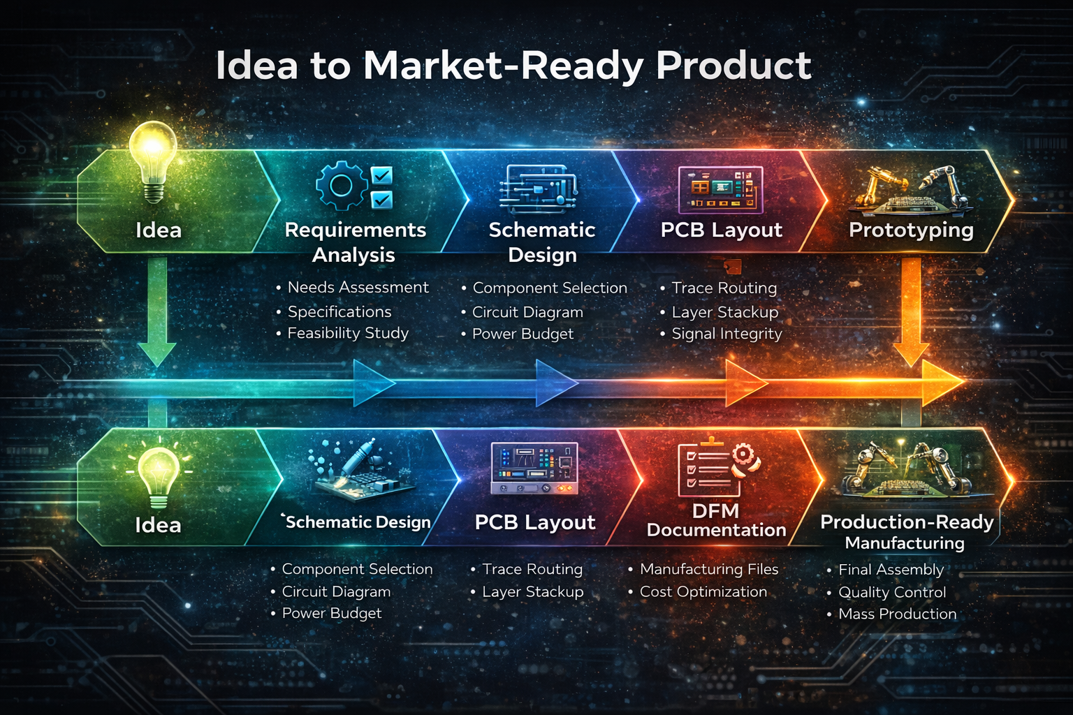
The journey from an idea to a market-ready solution requires a structured engineering and development process. Professional PCB Product Development Services ensure that each stage is executed with technical precision, reducing risks and improving long-term reliability. Every phase plays a critical role in transforming a raw concept into a manufacturable and commercially viable electronic system. Skipping or rushing any stage can lead to redesign costs, performance issues, or production failures. Below is a clear explanation of each stage in the Idea to Market-Ready Product process.
The first stage is the Idea phase, where innovation begins. The concept may originate from solving a real-world problem, improving an existing device, or introducing a new technological solution. At this stage, the purpose, target users, and expected performance outcomes are clearly defined. A strong idea phase focuses not only on creativity but also on market demand, technical feasibility, and long-term sustainability. Structured planning at this level lays the foundation for reliable electronic product development.
The second stage is Requirements Analysis. During this phase, the concept is translated into measurable technical specifications. This includes defining voltage ranges, current levels, environmental operating conditions, safety standards, size constraints, and cost objectives. Engineers evaluate feasibility, identify potential technical risks, and create a development roadmap. A clearly documented requirement plan prevents miscommunication and significantly reduces design revisions. High-quality PCB Product Development Services rely on this phase to align business goals with engineering execution.
Next comes Schematic Design, where the electrical architecture of the system is created. Component selection is based on voltage ratings, current capacity, reliability, thermal limits, and market availability. The circuit diagram defines how signals and power flow through the system. Protection mechanisms such as overcurrent protection, overvoltage protection, and thermal safeguards are integrated to enhance reliability. Simulation tools may be used to validate theoretical behavior before physical implementation begins.
The fourth stage is PCB Layout Design, where the schematic is converted into a manufacturable board design. Proper component placement, optimized trace routing, grounding techniques, and thermal management strategies are implemented carefully. High-current traces are calculated precisely to prevent overheating, while EMI and EMC considerations ensure stable signal behavior. Layout quality directly impacts performance, efficiency, and durability, making it one of the most critical stages in the overall development cycle.
The Prototyping stage follows layout completion. A limited batch of boards is fabricated and assembled for functional validation. Initial power-up is conducted in controlled conditions to avoid component damage. Engineers test voltage levels, signal behavior, load response, and temperature rise. This stage reveals practical improvements and ensures the design performs as expected before scaling to mass production.
After prototyping, Testing and Optimization are performed. The system undergoes load testing, thermal analysis, efficiency measurements, and stress evaluation. Necessary adjustments are made to improve performance stability, reduce electrical noise, and enhance overall reliability. This refinement stage ensures the final solution performs consistently under real-world operating conditions.
The next step is DFM and Documentation (Design for Manufacturing). The design is reviewed for production readiness. Parameters such as trace spacing, solder mask clearance, drill tolerances, and component layout are verified according to manufacturing standards. Fabrication files, including Gerber data, drill files, Bill of Materials, and assembly drawings, are prepared accurately. Professional PCB Product Development Services prioritize clear documentation to ensure smooth communication between design and manufacturing teams.
The final stage is Production-Ready Manufacturing. Once validation and optimization are complete, the design moves to bulk production. Assembly processes are standardized, quality control protocols are implemented, and inspection ensures consistency across batches. At this point, the system is ready for commercial deployment and market distribution.
Each stage in this structured framework builds confidence and minimizes risk. From initial concept evaluation to final production precision, the development process ensures technical excellence, scalability, and long-term reliability. By following a disciplined engineering approach, innovative ideas are successfully transformed into dependable electronic solutions ready for the marketplace.