Idea
→
Custom PCB
→
Tested Prototype
Idea-to-pcb-for-startups.Proven with 3-Step PCB Prototyping – Trusted Engineering for Startups & Industries
Idea-to-pCB for startups. Proven with 3-StepPCB Prototyping–Trusted Engineering
for Startups & Industries
At KIEE PCB, we transform innovative concepts into reliable, production-ready printed circuit boards through a structured and engineering-focused Idea to PCB development process. Every successful electronic product begins as an idea, but converting that idea into a stable, manufacturable PCB requires technical expertise, real-world experience, and careful planning. With over eight years of hands-on experience in PCB design and electronics engineering, we guide startups, manufacturers, and product developers through a systematic approach that ensures their concepts evolve into dependable electronic systems built for long-term performance.
Our Idea to PCB process begins with understanding your vision in detail. We analyze functional requirements, operating voltage and current levels, switching frequencies, environmental conditions, mechanical constraints, and cost targets. This early-stage evaluation allows us to identify potential design challenges and provide practical technical recommendations before circuit development begins. By establishing a strong engineering foundation at the start, we reduce unnecessary revisions and ensure smoother project execution.
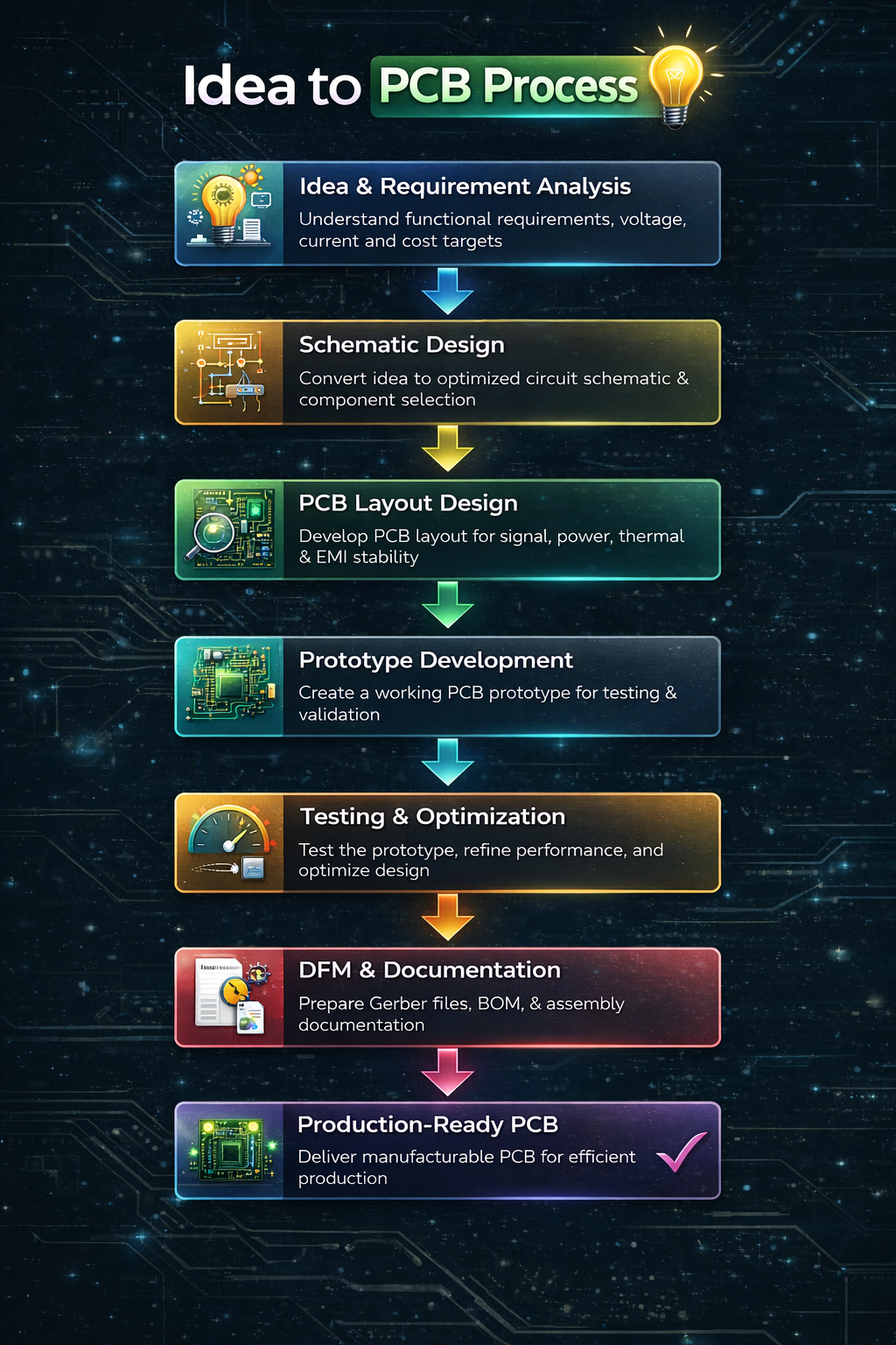
Once requirements are clearly defined, we move into schematic design and circuit architecture development. This phase translates your idea into a logical and optimized electronic framework. Component selection is carried out with careful consideration of reliability, electrical margins, availability, and lifecycle stability. We ensure that all components are properly rated and integrated with appropriate safety buffers to support long-term durability. Protection circuits such as overcurrent protection, voltage regulation safeguards, and thermal considerations are incorporated wherever necessary to enhance system resilience.
After schematic validation, the project advances to PCB layout design, where performance and reliability are refined. PCB layout is a critical stage in the Idea to PCB process because it directly influences thermal behavior, electrical noise, signal clarity, and overall system stability. Our layout strategy prioritizes optimized component placement, efficient power distribution, controlled grounding architecture, and minimized loop areas to reduce electromagnetic interference. For high-current and high-voltage applications, we carefully calculate trace widths, copper thickness, and creepage and clearance distances to ensure safe and stable operation under demanding conditions.
Thermal management is another key factor in transforming an idea into a functional PCB. Many electronic failures result from poor heat dissipation or improper current handling. We integrate heat management techniques such as copper pours, thermal vias, and intelligent component placement to maintain safe operating temperatures. By controlling heat flow and minimizing localized temperature rise, we improve component lifespan and overall product reliability.
Manufacturability is central to our Idea to PCB philosophy. A design is only successful when it can be produced efficiently and consistently. We apply Design for Manufacturing principles during the layout stage to ensure smooth assembly and fabrication. Production-ready Gerber files, drill data, Bill of Materials documentation, and assembly guidelines are prepared with clarity and precision. This structured documentation minimizes manufacturing errors and ensures seamless communication between design and fabrication teams.
Our support continues beyond file delivery. We assist clients during prototype validation by reviewing testing results and recommending improvements where necessary. Early-stage refinements often enhance performance stability and reduce production risks. If design optimization or redesign is required, we provide structured technical guidance to ensure the final version is robust and scalable for commercial production.
The Idea to PCB service at KIEE PCB is suitable for industrial automation systems, power electronics projects, induction heating controllers, embedded systems, and custom electronic product development. We understand that industrial electronics operate under real-world stress conditions including electrical noise, fluctuating loads, temperature variations, and continuous operation cycles. Our designs are developed to handle these practical challenges with confidence.
What sets us apart is our commitment to engineering integrity and long-term reliability. We do not focus solely on achieving functional prototypes; we design PCBs that are stable, manufacturable, and built for sustained operation. Clear communication, structured workflow, and disciplined engineering practices ensure that every project moves from idea to finished PCB with precision and professionalism.
At KIEE PCB, we believe that every innovative idea deserves a solid electronic foundation. By combining practical experience with technical discipline, we convert your concept into a dependable printed circuit board that supports product success and long-term growth.